- Contact Person : Ms. Wu Maggie
- Company Name : Shanghai Panmeng Electronic Materials Co., Ltd.
- Tel : 86-21-3782-1572
- Fax : 86-21-3373-4521
- Address : Shanghai,Shanghai,Building A4,No.6638 Beisong Hwy,Songjiang District,Shanghai.
- Country/Region : China
- Zip : 201611
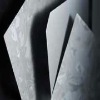
8"Mono Solar Wafer
Dimension | 125 mm | 156 mm |
Growth Method | CZ | CZ |
Conductive Type | P | P |
Dopant | Boron | Boron |
Orientation | <100> | <100> |
Off Orientation | <±2° | <±2° |
Resistivity | 1 –3 Ω•cm | 1 –3 Ω•cm |
Bulk Lifetime | ≥10μs | ≥10μs |
Oxygen Content | ≤1.0*1018 /cm3 | ≤1.0*1018 /cm3 |
Carbon Content | ≤5.0*1016 /cm3 | ≤5.0*1016 /cm3 |
Dimension | 125*125±0.5mm | 156*156±0.5mm |
Diagonal | 150±0.5mm | 200±0.5mm |
Square Sides Angle | 90±0.3° | 90±0.3° |
Streight Sections Length Deviation | 29.76±1.0mm | 21.81±1.0mm |
Thickness | 200±20 μm(thinnest≥180μm) | 200±20 μm(thinnest≥180μm) |
TTV | ≤30μm | ≤40μm |
Saw Mark | ≤15μm | ≤μm |
Warp | ≤50μm | ≤70μm |
Chips | Depth<0.3mm;Length<0.5mmless than 2pcs | Depth<0.3mm;Length<0.5mm,less than 2pcs |
Appearance | No Stain, No Pinhole and Cracks byVisual Inspection | Have slight saw mark and surface chip |
Dislocation Density | ≤3000 pcs/cm2 | ≤3000 pcs/cm2 |
8"Mono Solar Wafer